FPA
JSS component is missing React implementation. See the developer console for more information.
Defining Possible in Microelectronic Technology
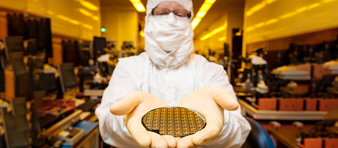
Northrop Grumman is a leader in designing, fabricating, packaging and delivering discriminating microelectronics to the military, aerospace, and commercial markets. For more than 50 years, we have been offering a wide range of trusted foundry and semiconductor services that deliver high performing and reliable microelectronics. Our wide breadth of technologies and capabilities allows us to provide our customers with unique “More than Moore” solutions.
- SENSING: Microelectronics allows connections of sensors and shooters utilizing materials specified to the mission.
- SECURITY: Being a trusted domestic foundry, Northrop Grumman ensures our microelectronics are protected and created for advanced warfighting capabilities, specific to our national security.
- COMPUTING: Processing digital information, transferring, transporting, organizing and translating data so that mission critical decisions can be made.

Advanced Technology Lab (ATL)
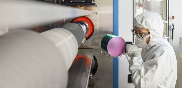
The Northrop Grumman Advanced Technology Lab (ATL) foundry, located in Linthicum, Maryland, maintains a wide range of processes for both internal and external customers.
Products
ATL offers foundry services in both Silicon and Compound technologies. Our standard products encompass Radiation Hardened Memories, ASIC’s, and Power Transistors.
Micro-Line
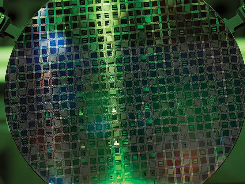
The μ-Line, located in Apopka, Florida, establishes a wafer post-processing and test source tailored for defense applications.
Products
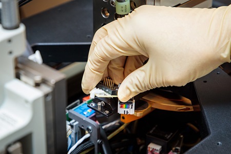
The μ-Line offers a complete suite of back-end wafer post-processing capabilities, including passivation, solder bumping, dicing, advanced inspection and test for up to 300 mm (12 inch) wafers.
Space Park
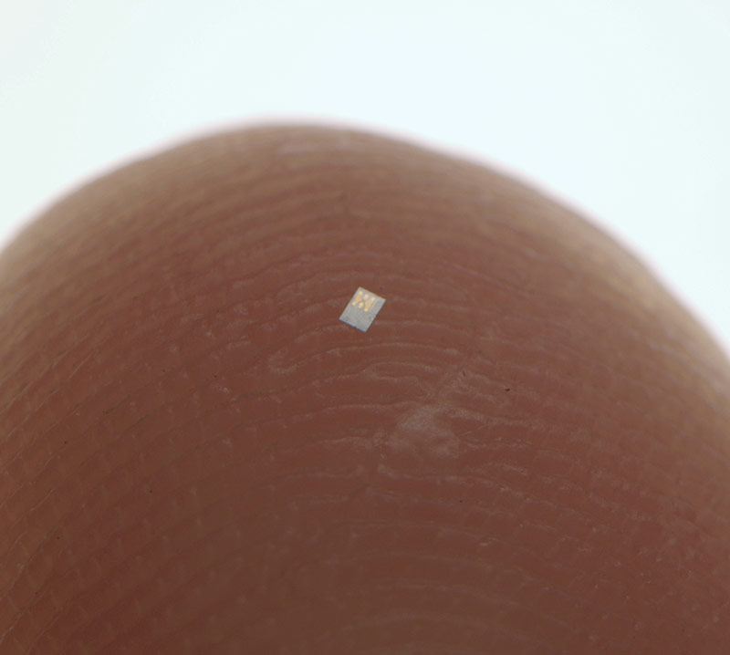
Our Space Park foundry offers products for E-Band (71-86 GHz) Wireless communication; W-Band (> 86 GHz) applications; millimeter-wave imaging at 80-100 GHz; and W-Band communication for challenging military and commercial wireless, high-power amplifier applications.
